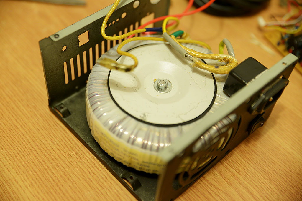
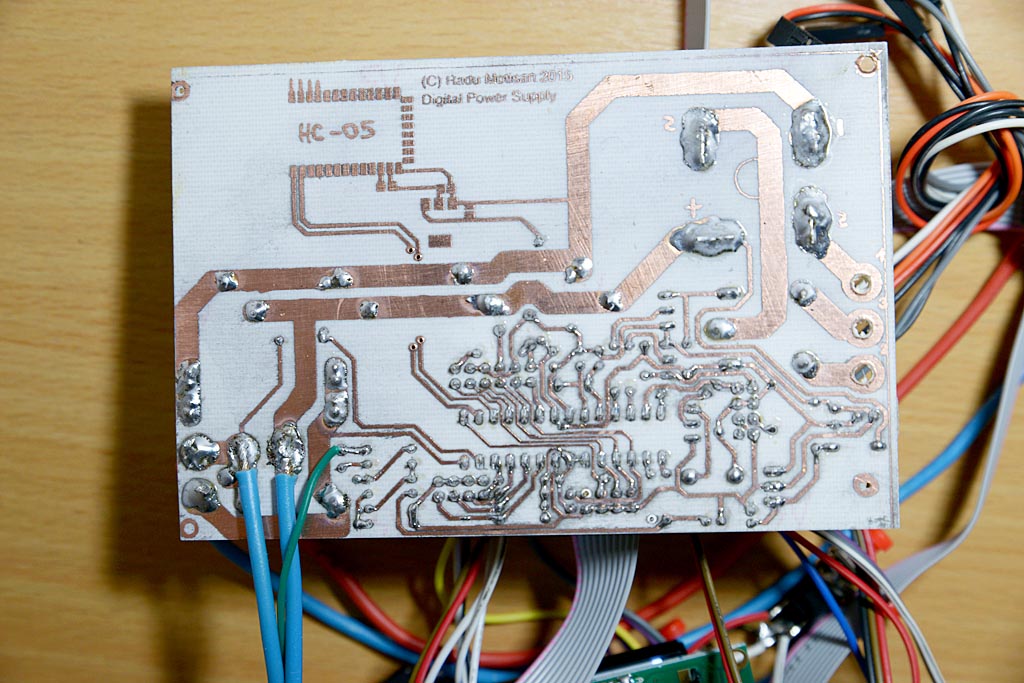
As a follow up to one of my earlier projects, the Variable regulated power supply, initially designed to deliver 0..30Volts at up to 10Amps, I have decided it was time for an upgrade. I kept the enclosure and the nice 250W toroidal transformer, and am reshaping everything as a new digital power supply with regulated voltage and current, short circuit protection, lcd display, buzzer for various alarms, temperature sensor on the heat sink and automated protection. Optional bluetooth (HC-05 module) connectivity has been added to the PCB, to allow programming the supply or reading its parameters. For the core of this design I’ve chosen the well known ATMega8 microcontroller.
I’ve built this from scratch, so I wanted to explain all steps properly. The article got rather large in length, so you might want to use the following table of content to jump directly to the section of interest:
01. Introductory details
02. The working principle
03. The Digital to Analog Converter (DAC)
04. Voltage amplifier using an OP-Amp
05. Controlling the output
06. The user interface
07. Pictures and comments
08. Source code and PCB
09. Final notes
01. Introductory details
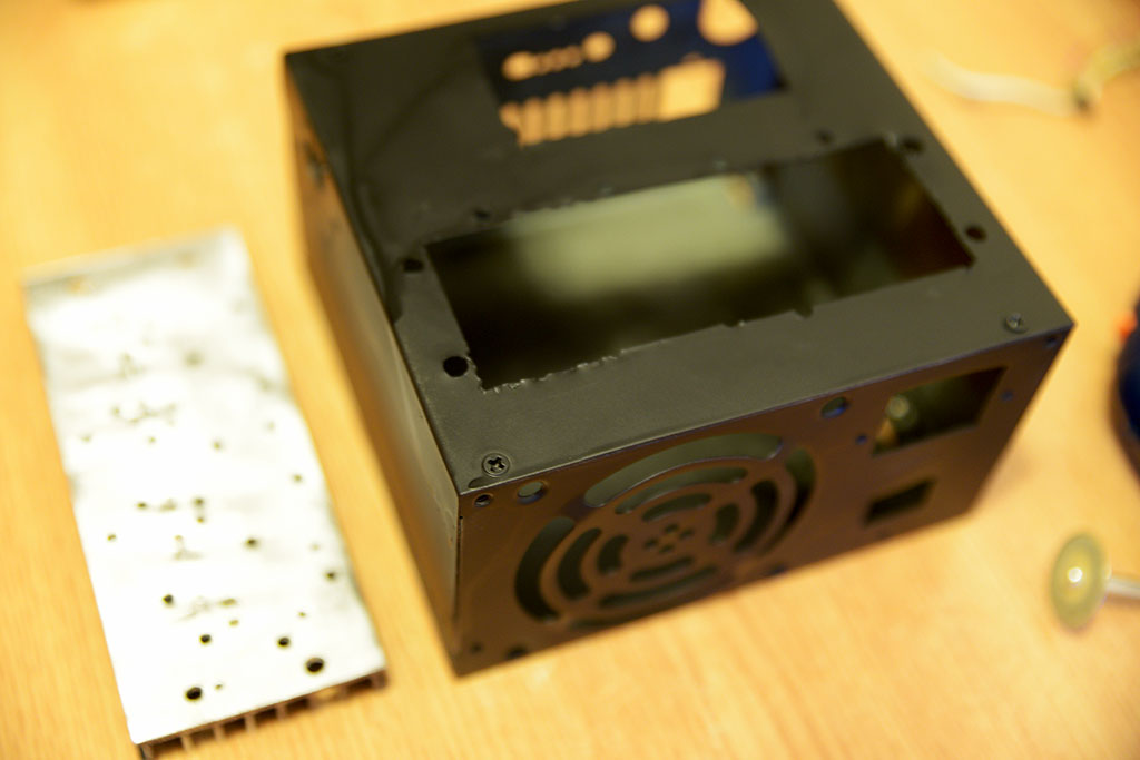
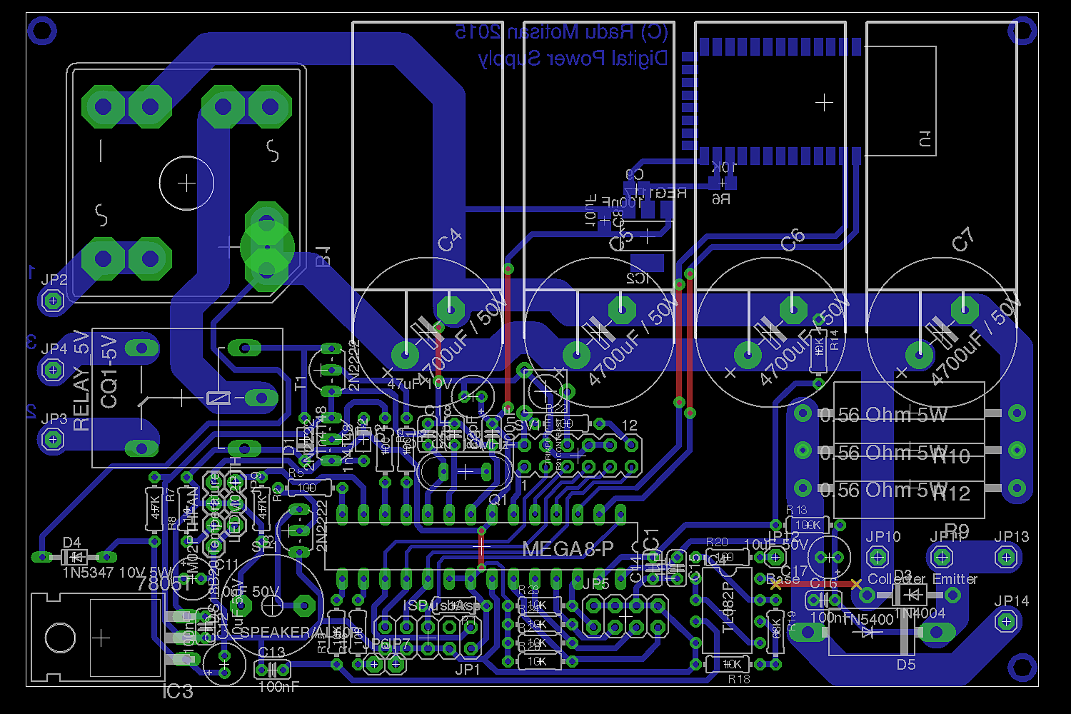
The enclosure has been brushed using a rotary tool, than painted black with a nice opaque colour. The heat sink has been cleaned and the power transistors mounted using wood screws that work great with aluminium as well.
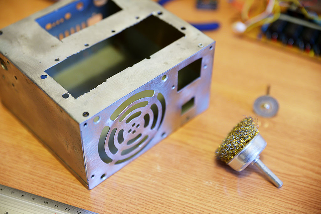
A DS18B20 temperature sensor is also added to the heat-sink and pressed tightly using a metal piece for optimum contact. It’s purpose is to start the fan or cut the power off depending on how hot it gets.
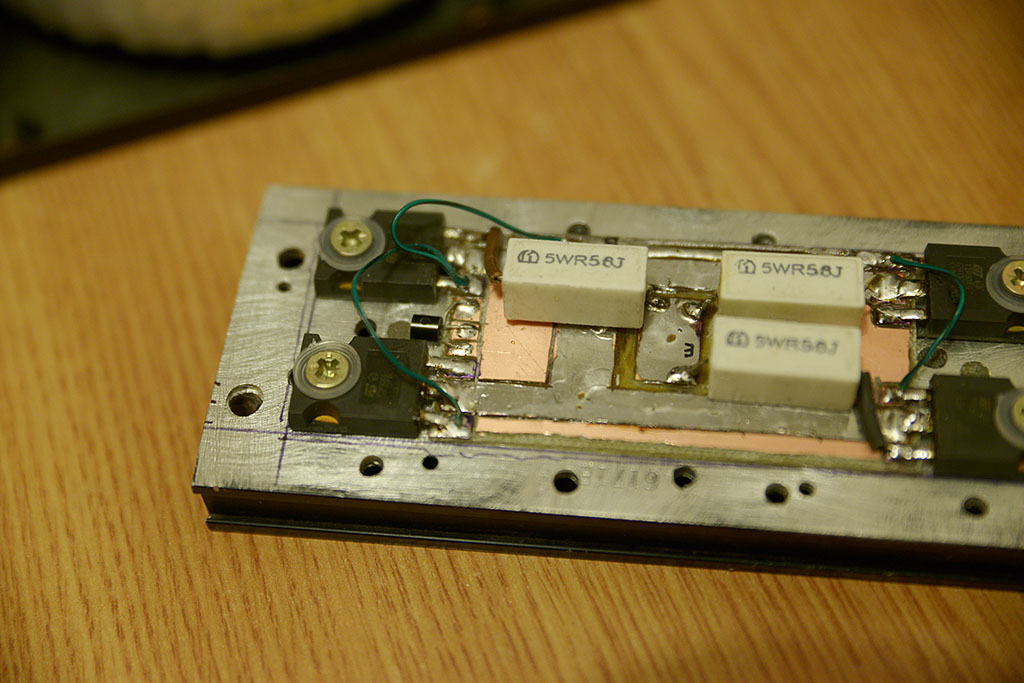
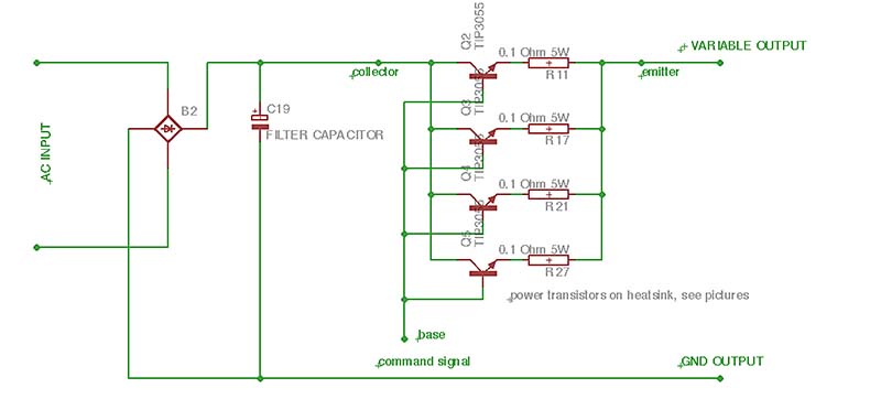
The resistors in the pictures have been changed to 0.1Ohm 5W, in the final circuit diagram. They are connected one to each transistor’s emitter, to equalise the current trough this parallel assembly.
02. The working principle
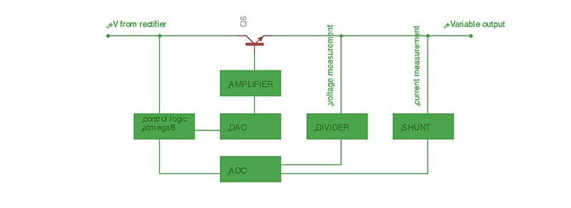
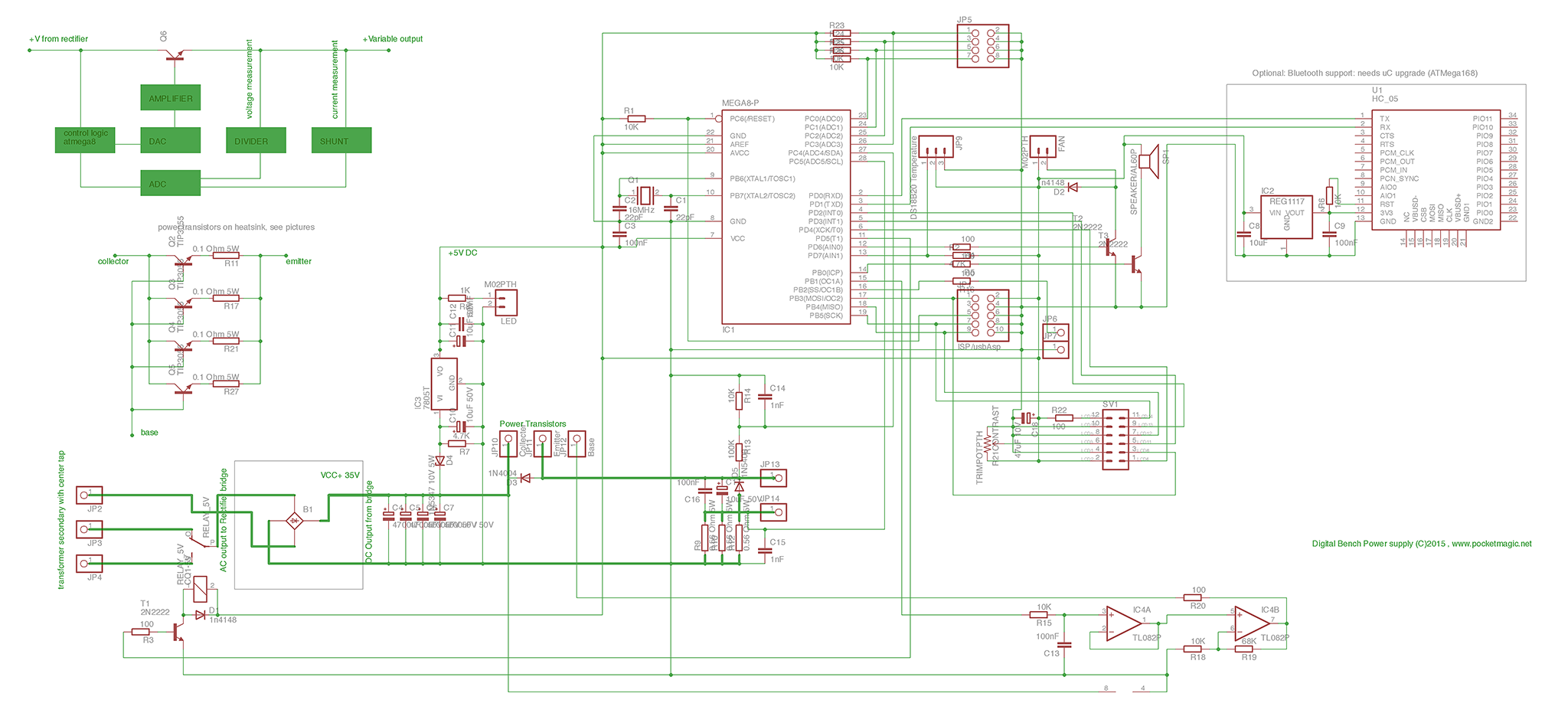
So we have the transformer, a rectifier bridge and a few filter capacitors. The output goes trough several power transistors mounted in parallel on the heatsink. All is left to do is to linearly control the base of the power transistors in order to get variable output. In my previous design I used the LM317 for that. Now, with the digital design, I designed a digital to analog converter (DAC) to serve the purpose.
A representative block diagram would be the following:
The transformer I am using puts out 24VAC and has a centre tap for 12VAC and is rated for 250W. After the rectifier and the filter caps, for the full 24VAC, I can measure an output of 33.8Volts. Ideally, the supply should give us a variable output from 0V to 33.8V at a maximum current of 10Amps, or at least as close to that as possible. For practical reasons, let’s set the target for the maximum output voltage to 30V.
03. The Digital to Analog Converter (DAC)
To command the base of the power transistors we’ll need a signal that goes from 0 to 30V. The Atmega8 has plenty of Analog to Digital converters, but not the opposite. So we need to build one ourselves. There are several options here. One is to use a dedicated IC. I had none in my toolbox. So to build everything from scratch, I could either go for a R-2R network or for using a PWM output with a low pass filter.
OPTION-1: DAC with a R-2R network
While being fast and stable, this requires lots of resistors and a high number of IO pins, depending on the maximum resolution we want to achieve. A solution to reduce the pins is to use a shift register, like I did on my serial digital to analog converter, but I simply didn’t have enough space on the PCB. So I went with the second option:
OPTION-2: DAC with a PWM generator and a low pass filter
Using ATmega’s PWM on port PB1, I can generate a variable duty cycle PWM signal. A low pass filter consisting of a resistor and a small capacitor is added.
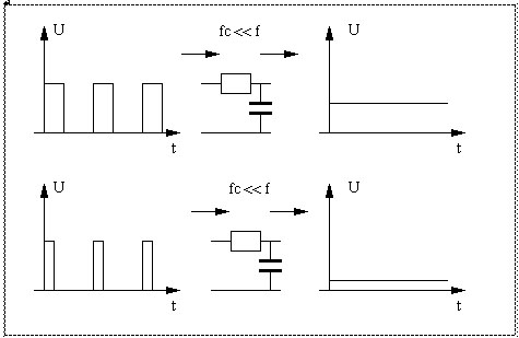
When the PWM signal goes high, it starts charging the capacitor, so the output voltage starts rising. When the PWM signal goes low again, it starts discharging the capacitor and the output voltage starts falling. The DC voltage at the output isn’t smooth, it keeps going up and down slightly around the average voltage, and effect called ripple. You can find more details on this in the Serial digital to analog converter article, under DAC Method 1.
By changing the duty cycle from 0 to 100%, we get a variable voltage on the filter’s capacitor which goes from 0V to Vcc, which for our circuit is 5V. To use a small size capacitor and save space on the PCB, the PWM’s frequency must be high. To get from 5V to 30V, an OP Amp is used between the DAC and the power transistors. The first half of the OP Amp works as a buffer, allowing the DAC signal in on its high impedance input, while the output is a low impedance one, perfect for controlling the bases directly. Before we get there, the second half of the OP Amp is used as a non inverting amplifier with a gain of 6 selected using resistors, to go from 5V to 6x5V = 30V, exactly what we need.
But to get back to the DAC, we need to keep an eye on the ripple, as that will get into our output line and affect the stability. Using the oscilloscope, I connected CH1 (yellow) on the filter capacitor and the second channel CH2 (cyan) on the base of the power transistors, right after the OPAmp output.
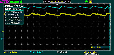
It’s not much, but it’s there. The question is what frequency works best for the smallest ripple? As the RC filter capacitor is 100nF, the answer is a higher frequency. Here is a comparison on the same setup, using 1KHz, 10KHz, and 100KHz. The first two oscillographs have identical bases (you can see all parameters at the bottom):
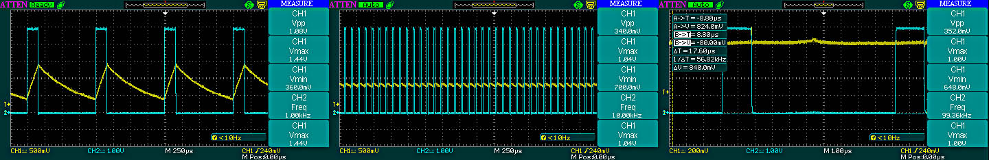
Going with 100KHz reduces the ripple on the output to less than 0.05V. The DAC is ready.
04. Voltage Amplifier using an OP-Amp
If you want to learn what an op-amp is, see Dave’s video tutorial – by far one of the best resources on this topic:
Having the DAC output 0 to 5V, an OP-Amp was the perfect choice for boosting the command signal to 30V. There are certain limitations and if you’ve watched the video you know the OPAmp output can’t really reach the rails input, unless it was designed to do so. Regular OPAmps will have a few volts difference. If I use the TL082, this digital bench power supply will output 26V and a maximum current of 5Amps. If I use the LM384, the maximum output goes up to 31.5V, while the maximum current will only be little below 4Amps. I also tried the TL062 and the LF357 but the results where inadequate for this application.
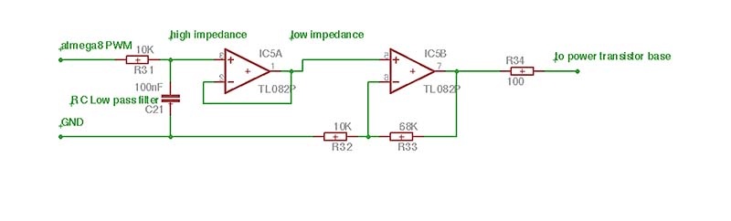
The diagram shows the way the OpAmp is used. The first half as a buffer, taking the DAC output on its nice high impedance input, and setting a gain of almost six (68K/10K = 6.8) to amplify the low DAC voltage up to the interval we want. The output is a low impedance one, perfect for driving the power transistor base directly. So this block will set certain limits on the design. I opted for the TL082 for the final variant.
The second half of the OPAmp receives feedback on its negative input via the 68K / 10K resistors. The gain will be A = 68K / 10K = 6.8 . The 100 Ohm output resistors has little effect on the limits the supply can reach, it is there just to protect the base of the transistors from over-current.
Note: the opamp’s rails are connected to the maximum voltage provided by the power supply, immediately after the rectifier block and to GND. This means two things: the opamp used must be able to withstand the relatively high input voltage, which in this case goes up to 33.8V . Second, as the negative rail is connected to ground, the voltage output is shifted to positive values only, but that is exactly what we want here. As Dave explained, even those opamps rated for dual positive/negative supplies will work in this configuration, assuming the difference from V+ to V- is greater then our requirement of 33.8V for this application. The TL082 fits ok, while the LM384 is pushed to the limit, but still works. Other Opamps can be used as well.
05. Controlling the output
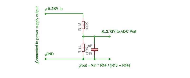
This supply needs to be regulated (controlled voltage and current) but also offer shortcircuit protection. Finally we want the output parameters displayed on the LCD (voltage and drawn current). To do so, we’ll need a way of measuring the output voltage and current. For the voltage, a simple resistive divider connected to one of the microcontroller’s ADC ports does the job:
For the current, I used three high power resistors in parallel, with a low total resistance (0.18Ohm), in series with the power supply output. Each resistor is rated for 5W, so we get a total of 15W when in parallel. Using P = I^2 x R , we get I = 9.12Amps max current capacity.
When a consumer is connected, it is practically put in series with our shunt resistor, so the current flows through the consumer, but the same current also flows through our shunt, causing a voltage drop that validates Ohm’s law: I = V / R. We know the resistance (0.18Ohm) and we can measure the voltage using another ADC port, allowing us to find out what the current is.
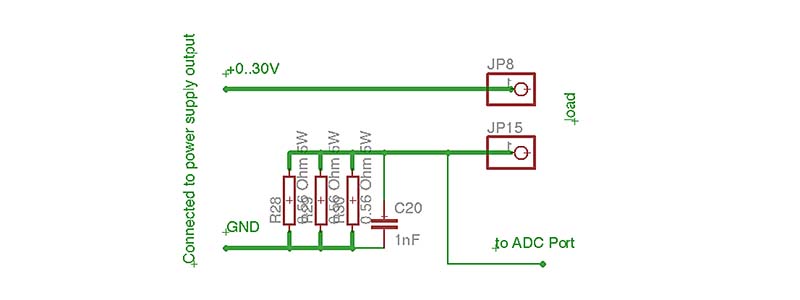
This means we’ll use one ADC channel for measuring the voltage and another ADC channel for measuring the current via the voltage drop on the shunt. Knowing the current is critical, so we can take action in case of shortcircuit. The ADC conversion must be done as quickly as possible and we need to react without any delays. This means the current control code must be done separately from the main program loop. The solution is to do the ADC conversions using interrupts, and set the prescaler to a convenient value. Each time the ADC conversion is complete, we change the channel (if it was voltage we go for current and vice versa) and we restart the ADC. By doing so we alternatively measure both the voltage and the current .
float vref = 5.0;
#define MODE_MEASURE_CURRENT 0
#define MODE_MEASURE_VOLTAGE 1
volatile bool adc_mode = MODE_MEASURE_CURRENT;
volatile float current = 0, voltage = 0;
...
// setup ADC to measure as interrupt: go for current first
adc_mode = MODE_MEASURE_CURRENT;
ADMUX = PC5;
ADCSRA = (1<
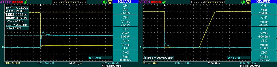
Even if half of the ADC conversions are "wasted" on voltage measurements, we still get a very quick shortcircuit response:
And here are some nice oscillographs showing the quick recovery after a shortcircuit event. It takes less than 350ms to recover to the original voltage configured as shown in the second picture. The CH1 (Yellow) is connected to the output, and the CH2 (Cyan) is connected to the shunt. The first picture shows the quick voltage drop on output, and an increase on the shunt, as expected.
Having the voltage and current precisely calculated, the next question is how to control the output? We use the duty cycle of the PWM generator for both!
If the digital bench power supply puts out more volts then selected, we decrease the duty cycle until we hit the target. Or the opposite case. For the current the same thing, again, thanks to Ohm's law applied on the load's resistance. But the order is important:
Right after the ADC measurements are done, and the voltage and current values saved in global volatile variables, first thing to check is the shortcircuit condition: a current considerably bigger than the limit. If we're in short circuit, the duty cycle is immediately reduced to compensate the risk factor. Then we get to check all the other cases. Why is this order important? If we were to adjust the voltage first, in case of shortcircuit we would see the voltage drop, and try to increase it back to where it was by pushing more power and incrementing the duty cycle, instead of prompt action of shutting the power down to save the power transistors from total destruction. The logic order makes a big difference!
The following code is done in the same ADC Interrupt call, due to it's maximum time-critical importance:
...
// control operations, in order
// 1. act on short circuit
// decrease quickly on current spike
if (current > targetCur + targetCur / 2) {
pwm.setDuty(pwm.getDuty() / 2);
alarm = true; // will sound alarm in main thread
}
// 2.act on over current
// decrease slowly on higher current
else if (current > targetCur) {
pwm.setDuty(pwm.getDuty() - 1);
}
// 3.act on over temperature
else if (tempval > TEMPERATURE_SHUTDOWN) {
pwm.setDuty(pwm.getDuty() - 1);
alarm = true;
}
// 4. act on over voltage
// take care of voltage with lower priority
else if (voltage > targetVol) pwm.setDuty(pwm.getDuty() - 1);
// 5. act on under voltage
else if (voltage < targetVol) pwm.setDuty(pwm.getDuty() + 1);
}
The temperature is also checked and we reduce the power output by decrementing the duty cycle, in case the supply is too hot, to prevent damage. The speaker becomes useful for adding an alarm sound. The alarm is triggered by setting a variable and played in the main program loop, to avoid unnecessary and non-critical delays in the interrupt code.
I've been using a transformer with a center tap and a relay commutes the input automatically: either the center tap if the configured voltage is set to less than 12V, otherwise the full secondary. The relay is controlled automatically based on the target voltage. If you're using a transformer that doesn't have a center tap, just connect the AC input to pin 1 and 2.
There is also a FAN, that goes on when the heatsink becomes warm, to help with heat dissipation. Use a 5V fan or two in parallel.
06. The user interface
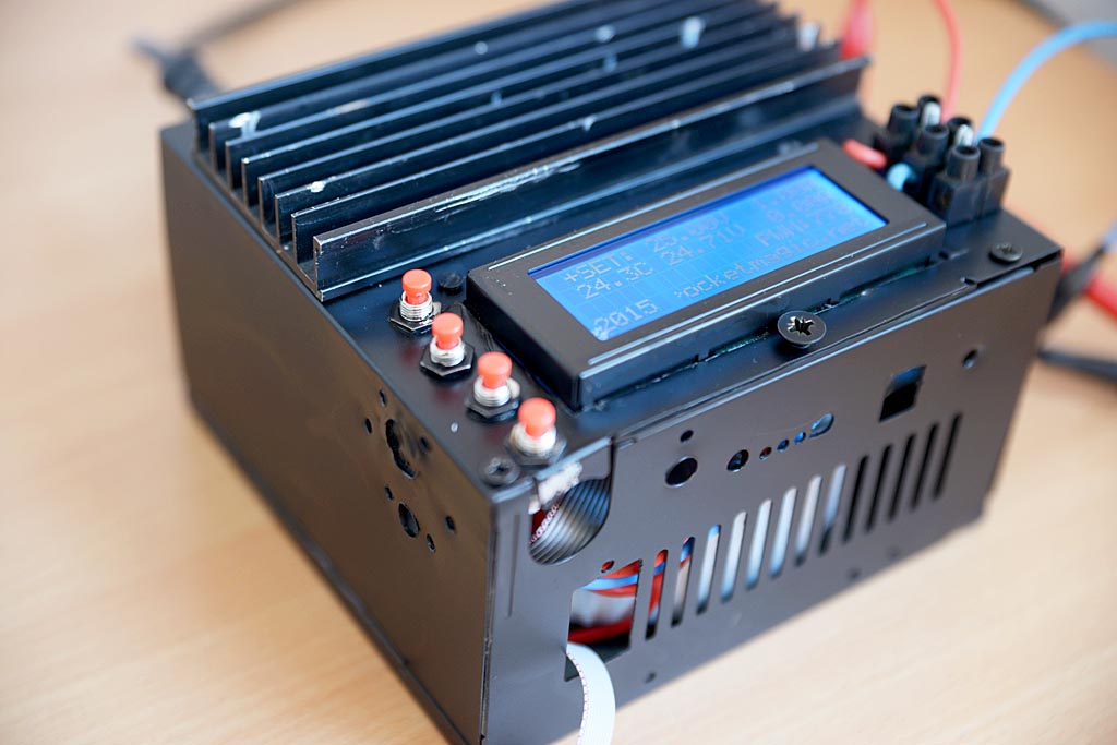
The display is a 4x20 characters HD44780 LCD, but you can go with a 2x16 as well.
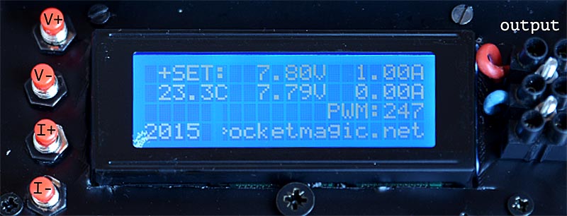
The first line shows the voltage and maximum current configured. The second line shows the measurements: temperature, voltage and current. The third line shows the duty cycle in per-mille (‰) . The last line is free, and I've added my blog's address there.
The four buttons are used to set the voltage and current. Two for the voltage - up and down in 0.10Volt steps, and two for the current in 0.10Amps steps.
The self oscillating buzzer used as an alarm, is also part of the user interface, by providing audible notifications. This is useful when our workbench is crowded (happens so often!) and errors are likely.
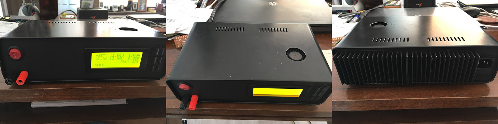
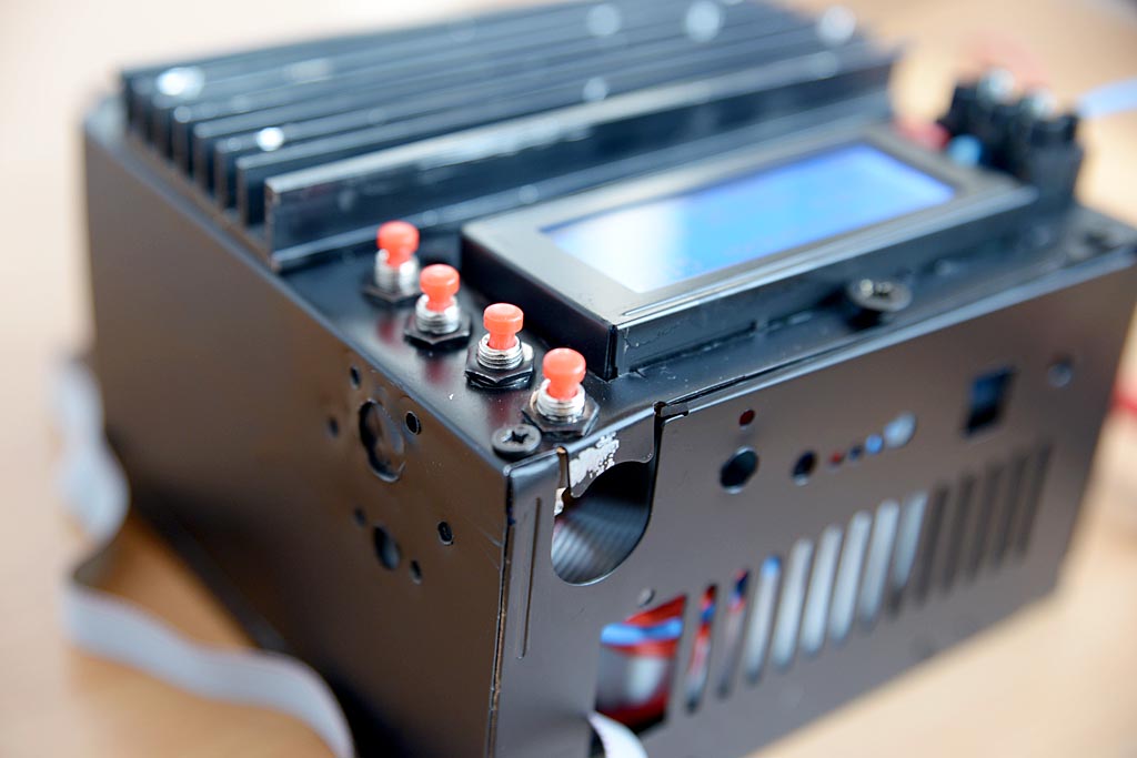
07. Pictures and comments
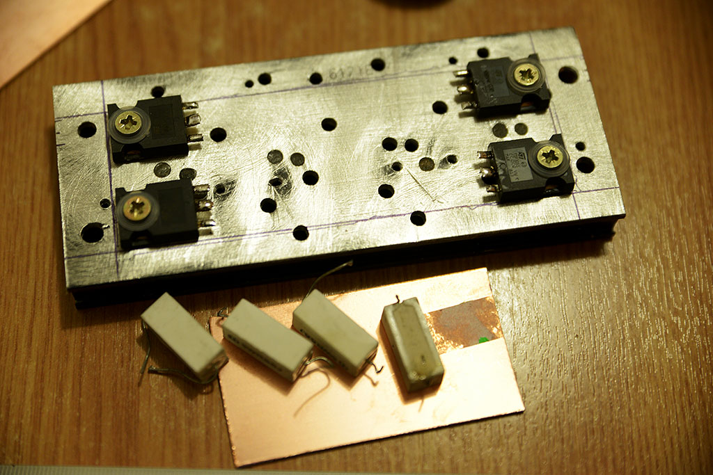
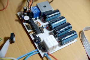
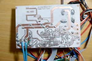
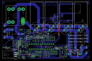
Time to see the final results. Here's the first prototype PCB, done with toner transfer method:
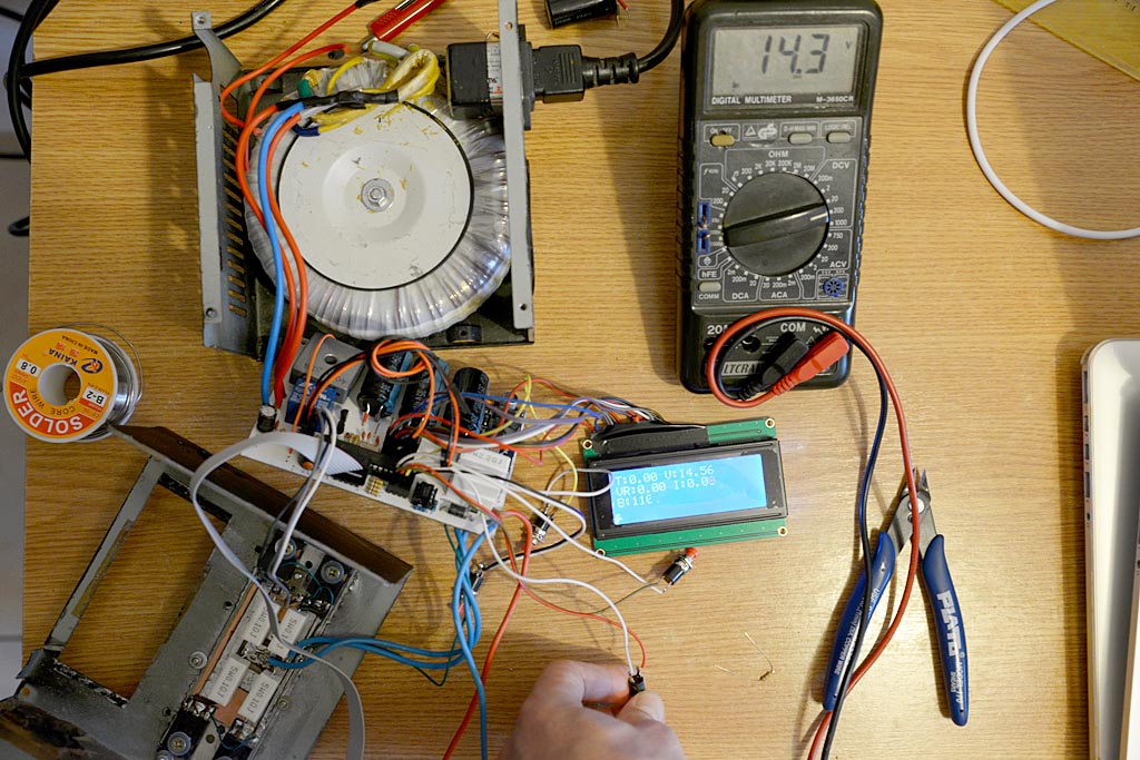
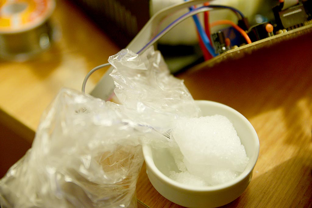
Here are a few tests, with the output control, the shortcircuit response speed tests, and even a few negative temperature tests for the DS18B20 code where I've used ice and salt to go below zero:
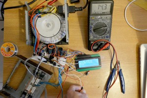
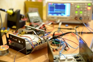

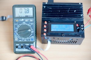
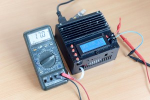
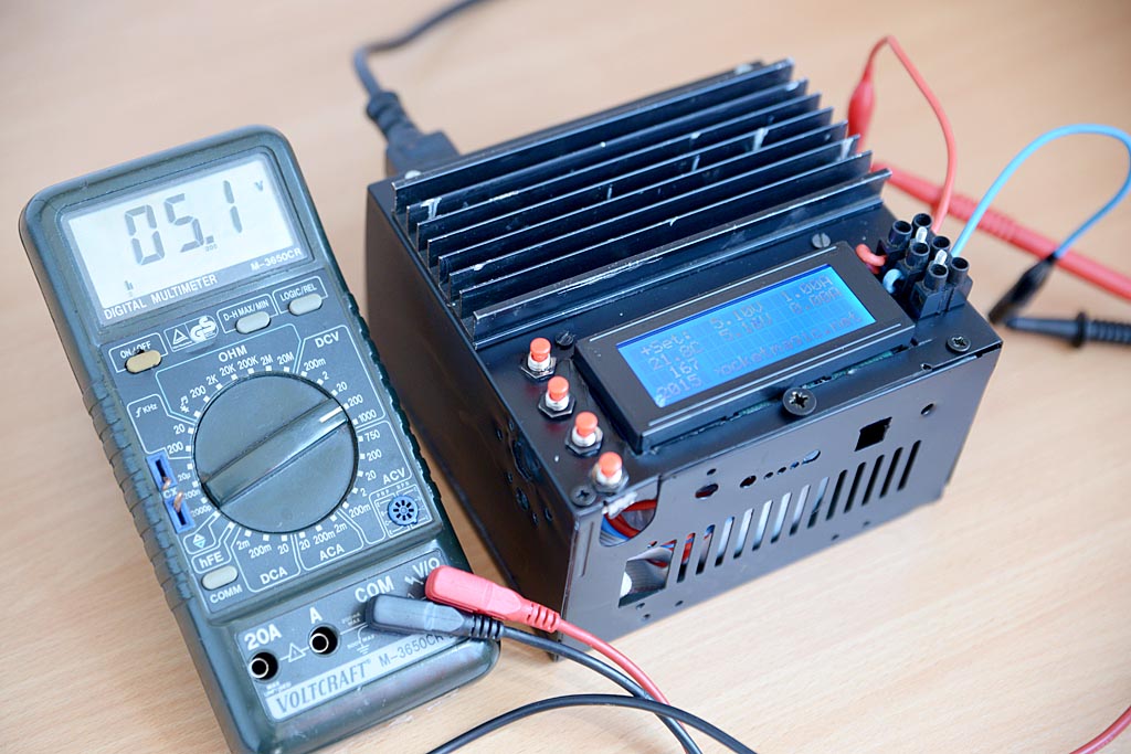
The multimeter was used in parallel, together with the oscilloscope, to confirm the output values as measured by the digital bench power supply:
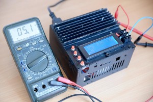
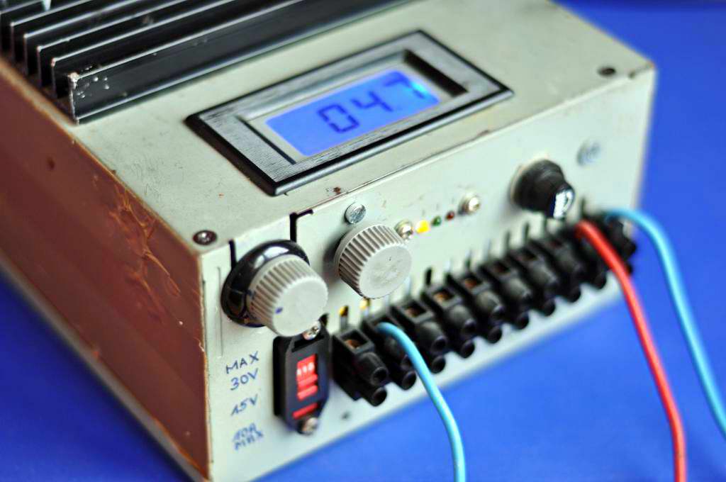
And last pics are reserved solely for the start of this article - the digital bench powersupply itself!
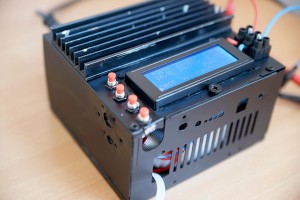


Yes, the last picture is the very old photo of my first power supply, constructed a few years ago. For any questions on this design, please use the comments section below or drop me a mail (my address is under the blog's About section).
08. Source code and PCB
This project is being released as open source, under GPL v2, hoping that it will be useful. Feel free to build your own variants, or even improve the design where possible. For any questions or feedback messages, use the comments form below.

This entire work has been released under GPL v2. It includes the circuit diagram as Eagle files, and the firmware source code. Revisions will be added from time to time, to fix bugs or bring enhancements. To review the GPL v2 license, click here.
Source code repos are available on Github or a first code release can be downloaded here.
BOM list: bom
09. Final notes
I just wanted to say thanks to all the great and knowledgable guys on elforum.ro who dedicated some of their precious time to contribute with suggestions to the development of this project.
Community variants
Daniel mailed me a few pics with his construction. Although he was a tough critic of his own work, I think his results are very nice:


Hi,
this is what I was looking for for a while. I was thinking about this first (http://www.tuxgraphics.org/electronics/201005/bench-power-supply-v3.shtml) but then I choose your design. Great project !!
I know I can get all parts from schematic, but can you publish BOM on the site ?
THX
Dan
Hi Dan, thanks.
I’ll put the BOM list together and add it to the article.
You can find the BOM list added to the article. Direct link: http://www.pocketmagic.net/wp-content/uploads/2015/04/bom.txt
Hi what compiler used for this project
Hello Vijaya,
I should have added this in the article. I used the Eclipse IDE with AVR Crosspack under OSX. It uses avrdude .
Cu ce as putea modifica ccodul sa il personalizez eu? daca scriu codul pe atmega 328 si pun blueetoth merge ? la ce ajuta bluetoothul sau care este rolul lui? transformatorul tau este 24 V sau 12-0-12 adica cu priza mediana?. adresa mea de mail este munteanu872@gmail.com
Mihai, daca bine am inteles intrebarea, vrei sa stii cu ce aplicatie poti deschide, edita si compila codul. Cum am raspuns chiar mai sus, am folosit Eclipse cu AVR Crosspack.
Codul se poate modifica usor pt mega328p . Poti sa adaugi si un modul bluetooth, dar acolo vei avea nevoie sa scrii si codul UART. Cu Bluetooth, ai putea sa afisezi parametrii statiei pe un smartphone, si sa faci reglajele tot de acolo. Dar pentru asta ai nevoie si de o aplicatie dedicata pentru Android / iOS. Eu nu am timp sa o scriu deci te descurci.
Trasnformatorul meu e 24 cu priza mediana, deci (0-12-24).
Multumesc pentru informatii , codul o sa il modific eu . ultima intrebare ar fi daca am transformatorul 0-12-24 V care este ordinea conexiunilor pe cablaj ca am acolo la conexiuni 1, 3 ,2 la 1 se conecteaza comunul , la 2 se conecteaza 12 V iar la 3 se conecteaza 24 V? . nu as vrea sa fac o prostie conectandule gresit . multumesc si bafta
Asa cum ai intuit, numerele sunt date in ordine si decrierea scrisa de tine e corecta. 2 e priza mediana.
I’ve translated your native language posts.
Well, the code is not so simple to port for ATmega328, many registers are different. Tried to do that, but I don’t have enough free time 🙁
It would be nice to have a port for mega328 as there’s almost no space left in mega8 for improvements.
I’ve builded it and got it finally running with mega8, but got some problems with calibrations.
Measured voltages displayed on LCD don’t match sometimes with multimeter. And setted voltage also.
Ie. setted 5v, LCD 5v, multimeter 5v.
Setted 5.20v, LCD 5.15v, multimeter 5.10v.
Setted 5.30v, LCD 5.25v (lets say its ok), multimeter 5.30v.
Some voltages match almost perfect, while some are more or less inaccurate.
Hi , glad you got it working – drop me a few pics with your setup so I can post them here.
I worked intensively both with atmega8 and atmega328 , so for me porting the code is not a problem. I will try to do that as soon as I get some time to revisit this project.
Radu
Hola amigo muy buen proyecto ,si fuera tan amable de indicar los pines del lcd y el voltaje del transformador.Gracias
Hi friend very good project, if you kindly tell LCD pins and voltage transformer. Thank you
Hi friend very good project, if you kindly tell LCD pins with ATmega 8. Thank you
Sorry, never used opamp before but is it correct that the gain on your schematic is 6.8? Because as per Dave’s video: gain=Rf/R1 + 1 so gain= 7.8?
Please correct me if i’m wronf.
This is a nice project, thanks a lot for sharing
Salut
Mestere te rog sa mai pui odata schema
Vreau sa o desenez in Eagle si nu se intelege nimic cind o mai maresc putin
Am inteles ( de pe elforum ) ca se poate cupla la un lcd 5110
o zi buna_super proiectul
salut Spark,
Ma bucur ca iti place. Vezi ca am dat deja sursele Eagle, in pcb/100 pe github, uite linkul direct: https://github.com/radhoo/digital_bench_power_supply/tree/master/pcb/100
Daca totusi ai nevoie de schema la rezolutie mai mare, e disponibila tot pe Github, uite linkul direct si pentru aceasta: https://raw.githubusercontent.com/radhoo/digital_bench_power_supply/master/circuit_diagram_sch.png
Pentru orice alte itnrebari, “feel free to get back to me” .
Hi,
1.check please files aux.cpp and aux.h in your repository. I can’t copy (move, edit, view….) this files !
2. I’ve try to compile it in AVR 4 with no success (not fit in mega8…..)
Q: any chance to use mega328 ?
THX
Dan
Hi Dan,
1.That’s because Windows is incapable of handling files named aux, lpt,com, etc . I strongly suggest migrating to Linux or MacOS.
2.Compile it using Eclipse + AVR plugin, or change the optimisation settings in your AVR4 to improve size
3.Feel free to use 328p instead of mega8.
Radu
Hi,
I just make it “work” in AtmelStudio 6.2 !! But those two file are still “locked” 🙂
Great! Feel free to share your solution for other users with Atmel Studio.
1. I’ll stick with Windows for this . I’m also using unix-like PC’s in my home 🙂
I renamed aux.cpp and aux.h to other files and use it in project 🙂
2. I don’t want to install another IDE so as I mentioned I made it work under AVR Studio 6.2 It was easy !!
3. My question about m328 was related to your post from July 10, 2015 at 10:03 am, that you will build it for this MCU 🙂
BTW: I’m close to finish this project (with some HW cjanges) very soon !! THX !
Dan
Quick question: What is JP6(PB2) and JP7 for ?
output command pin, reserved for future use.
THX
Dan
BTW aux.cpp and aux.h are not used anyway in this project !! 🙂 You can delete them ! 🙂
Hi Radu. I build this PWS with some HW changes. Atmega16, encoder for setting Voltage and Current, 12V relay, 12V fan, extra 12V on transformer for logic and relay(fan) …
So now I’m in the phase of testing it. It is running, but I have some problems.
1. TL082 does not work for me. I’v tried 4 pieces but non of them works. I always got full OPAMP supply voltage on the buffer output. Does not matter what was the PWM after the low pass filter (this changed OK!!). So I used LM358 and everything is OK.
2. Output voltage is not stabile. It’s flying +- 250mV, also PWM value is not stabile. Maybe the PWM frequency is too high ?
According my calculation it is almost 100KHz. Is it correct ? And the TOP value is 160.
Any idea where I can look for bug ?
THX
Dan